On June 26, 2024, SEMI-e The 6th Shenzhen International Semiconductor Exhibition opened at the Shenzhen World Exhibition & Convention Center. Featuring three exhibition halls and six major zones, the exhibition brought together 815 exhibitors and saw an exceptionally high attendance on its first day.
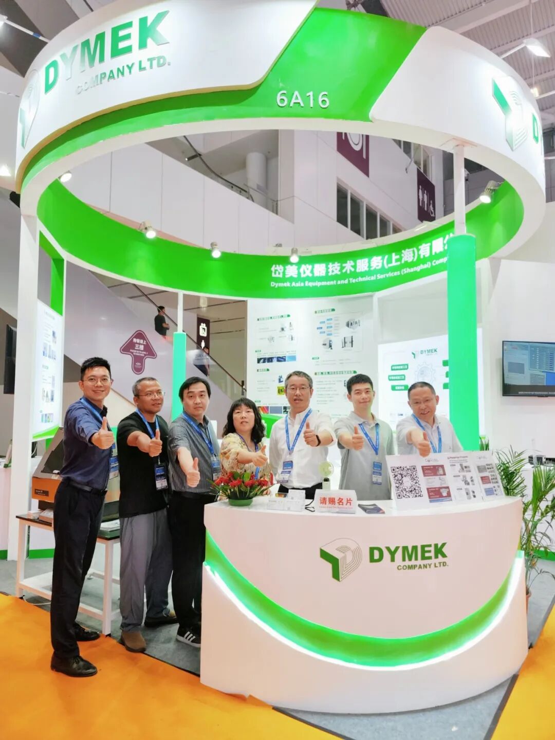
As an advanced semiconductor equipment distributor, Dymek China was honored to participate in this event.
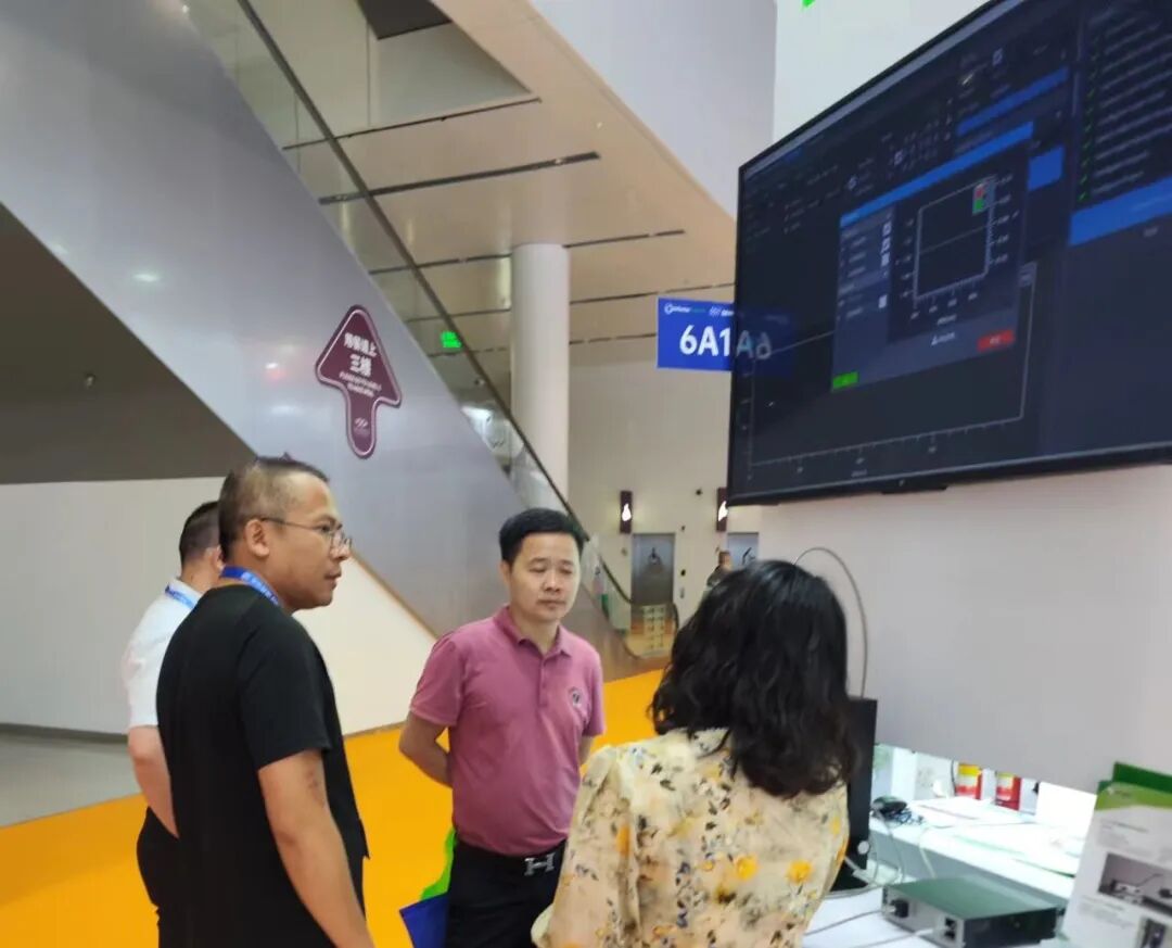
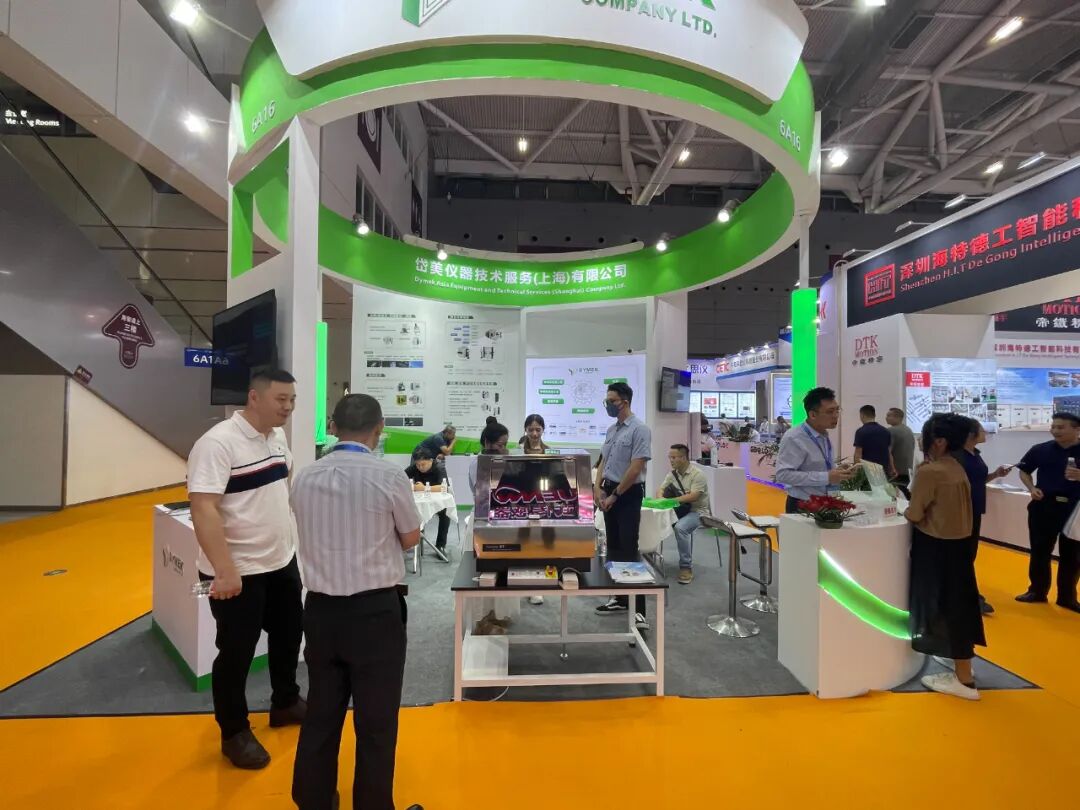
The exhibition gathered numerous industry experts and leaders, offering rich and insightful content. Dymek engaged in in-depth exchanges with peers, scholars, and entrepreneurs within the industry, sharing professional experiences and discussing the latest technology trends, gaining valuable insights and inspiration!
As a highly influential professional semiconductor exhibition platform, SEMI-e Shenzhen International Semiconductor Exhibition brought together 815 exhibitors, including industry leaders such as Hua Tian Technology, Shanghai Huali, Zhonghuan Leading, Tongfu Microelectronics, and HAJING Semiconductor, who made prominent appearances. The event comprehensively showcased the latest technologies and products across the semiconductor industry.
In addition to the dynamic exhibition, multiple themed summits were held. At events such as the “Semiconductor Industry Technology Summit,” the “Third-Generation Semiconductor Industry Development Technology Forum,” and the “2024 China Automotive Semiconductor Conference,” experts and senior executives from Huawei, Tianke Heda, NAURA, the 45th Research Institute of China Electronics Technology Group Corporation, Great Wall Motors, Dongfeng Company R&D Center, Tsinghua Unigroup Tongchuang, Keyou Semiconductor, and Basic Semiconductor shared insights on advanced semiconductor manufacturing and packaging technologies, as well as the latest application solutions for silicon carbide (SiC).
In recent years, third-generation semiconductor technology has gradually become a core driver in the semiconductor industry. As a pioneer in this field, we have accumulated extensive experience in meeting diverse inspection and metrology requirements for substrates and epitaxial wafers. To better understand and address customer needs, we have conducted extensive and in-depth exchanges with numerous customers, exploring the applications and development directions of various inspection and metrology technologies.
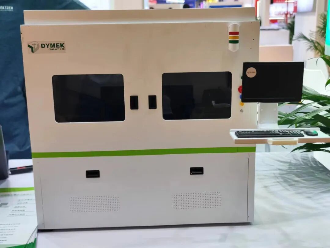
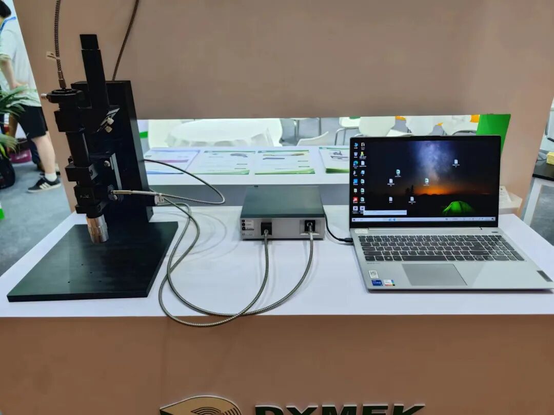
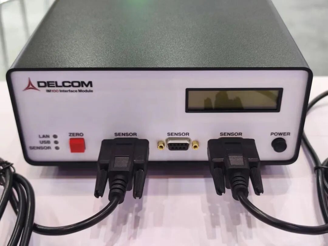
During these exchanges, we focused on several key inspection areas, including film thickness measurement, wafer thickness measurement, wafer topography measurement, wafer bonding, lithography, plasma cleaning, stress measurement, and sheet resistance measurement. Each inspection step is critical, directly impacting the performance and reliability of semiconductor devices.
Through these extensive and in-depth discussions, we have not only deepened our understanding of customer requirements but also driven continuous optimization of our own technologies and solutions. We remain committed to providing customers with the highest quality products and services, supporting the robust development of third-generation semiconductor technologies.