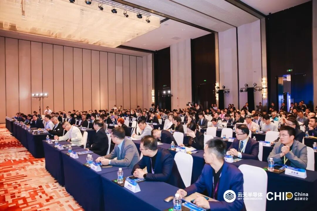
On November 28, 2024, the “2nd Semiconductor Advanced Packaging and Testing Industry Technology Innovation Conference” officially opened at the Haimen Regent Huayu Hotel in Xiamen.
The conference was co-organized by Xiamen YunTian Semiconductor Technology Co., Ltd. and Xiamen University, supported by the Xiamen Integrated Circuit Industry Association, organized by Asia ECS, and sponsored by the Agricultural Bank of China, Xiamen Branch.
Spanning two days, the event featured over 34 technical presentations covering key topics such as through-glass vias and related materials & equipment, 3D stacking advanced packaging, and advanced packaging process training. It brought together academic leaders, industry pioneers, and R&D managers for in-depth exchanges and collaboration, attracting nearly 500 attendees.
The exhibition area also hosted numerous leading companies, including NAURA, Huada Electronic Design, Zhi Cheng, ACM Research, PARK, Suzhou Jiazhi Color, CETC, Dymek, Rehm Thermal Systems, and Unionchem, among others. These companies showcased their latest technologies and products, comprehensively presenting the cutting-edge advancements and emerging trends—the “new pulse”—of the semiconductor advanced packaging and testing industry chain.
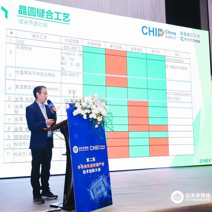
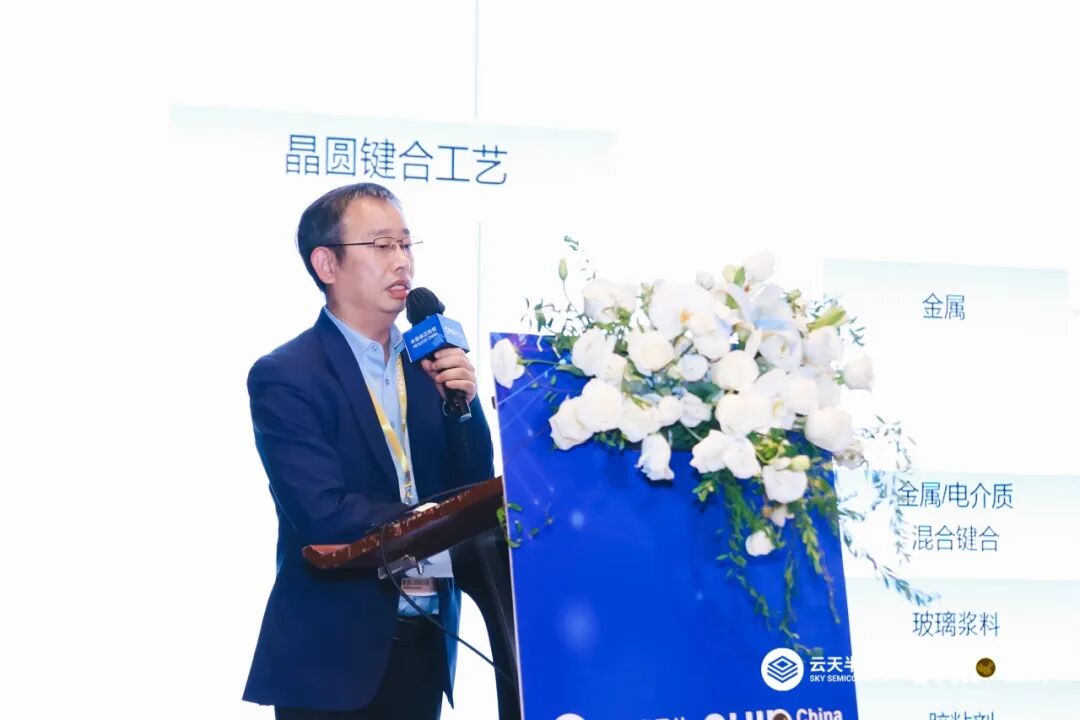
In the compound semiconductor supply chain, the manufacturing of semiconductor materials has always held a critical position. Traditional compound semiconductor materials are characterized by high manufacturing complexity and high costs. However, wafer-level bonding technology offers a convenient way to integrate different materials, enabling the creation of new composite materials that combine low cost with high performance. This approach is also compatible with existing semiconductor processes, improving yield while simultaneously reducing production costs, making it one of the key development directions for advanced compound semiconductor materials.
Through Dymek’s direct bonding processes and equipment, strong covalent bonds can be formed between different materials. The bonded wafers are fully compatible with subsequent manufacturing steps, thereby enhancing product performance and market competitiveness.
Dymek has always been committed to deepening its expertise in the semiconductor equipment field and continuously driving the iteration and upgrading of new products. Looking ahead, Dymek will stay attuned to industry development trends and evolving market demands, remaining focused on innovation and breakthroughs in semiconductor equipment technology.
We sincerely invite all our partners to join us in creating an even more brilliant future! We look forward to reuniting with you at next year’s events, to jointly explore new opportunities and achieve greater success together!