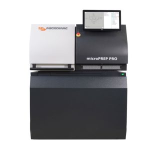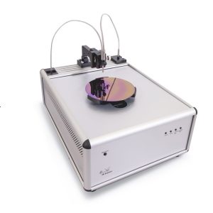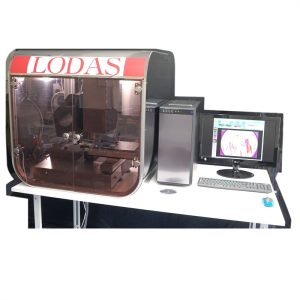

AutoWafer pro is our most advanced ultrasonic equipment for detecting defects in bonded wafers in a production environment, providing fast, high-resolution scanning of 200mm and 300mm bonded wafers.
A flexible, automated wafer inspection system designed for production, AutoWafer Pro provides fast, high-resolution scanning of 200mm and 300mm bonded wafers. It’s the ideal ultrasonic equipment for identifying bond defects in wafer applications such as MEMS, BSI Sensors, CMOS, memory, TSV and LED.
With extensive analysis capabilities at both the wafer and device level, there’s no need to reload and rescan wafers to get all the diagnostic images you need. And with high-speed scanning managed by fully automated wafer handling, AutoWafer Pro supports 100% nondestructive testing (NDT) for improved yields and a faster time to market.
By joining hands and leveraging cutting-edge technologies, we develop innovative solutions to drive societal progress and shape a better future.
With deep expertise and extensive experience, we deliver precise and efficient solutions to ensure every project meets the highest standards.
We integrate cutting-edge technology with continuous innovation to develop breakthrough solutions that drive industry progress and create lasting value for our clients.
We offer round-the-clock premium support services, ensuring rapid response and efficient problem resolution, allowing you to focus on your core business without worries.