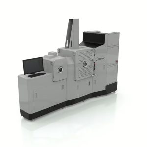
Beneq Transform® is an ALD cluster tool designed for technology development and manufacturing across power electronics (SiC, GaN, Si), RF, optoelectronics, microLED, MEMS, and sensors. Built for volume production, Beneq Transform scales with throughput and application requirements. It is an ideal platform for applications requiring surface engineering such as surface passivation of wide-band gap materials.
By joining hands and leveraging cutting-edge technologies, we develop innovative solutions to drive societal progress and shape a better future.
With deep expertise and extensive experience, we deliver precise and efficient solutions to ensure every project meets the highest standards.
We integrate cutting-edge technology with continuous innovation to develop breakthrough solutions that drive industry progress and create lasting value for our clients.
We offer round-the-clock premium support services, ensuring rapid response and efficient problem resolution, allowing you to focus on your core business without worries.