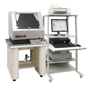

The ET200A, based on the Windows operating system, provides comprehensive surface morphology analysis for a wide range of materials, including semiconductor wafers, solar silicon wafers, thin-film heads and disks, MEMS, optoelectronic devices, precision-machined surfaces, biomedical components, thin films/chemical coatings, flat panel displays, and touch screens. It utilizes a diamond (hard probe) contact measurement method to achieve highly accurate surface topography analysis.
The ET200A reliably and precisely measures various surface morphology parameters, such as step height, roughness, waviness, wear depth, and thin-film stress.
Equipped with multiple types of probes, the system offers probe heads with controlled contact force and adjustable vertical range. The system also features a color CCD in-situ imaging design, allowing real-time observation of the probe’s working status for more accurate and convenient positioning of the test area.
| Max. sample size | φ160 × t 48 mm |
|---|---|
| Repeatability | 1 σ 0.3 nm or less |
| Measuring range | Z: 600 μm X: 100 mm |
| Resolution | Z: 0.1 nm X: 0.1 μm |
| Measuring force | 10 μN to 500 μN |
By joining hands and leveraging cutting-edge technologies, we develop innovative solutions to drive societal progress and shape a better future.
With deep expertise and extensive experience, we deliver precise and efficient solutions to ensure every project meets the highest standards.
We integrate cutting-edge technology with continuous innovation to develop breakthrough solutions that drive industry progress and create lasting value for our clients.
We offer round-the-clock premium support services, ensuring rapid response and efficient problem resolution, allowing you to focus on your core business without worries.