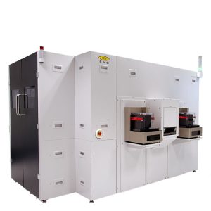

Versatile manual wafer bonding system for academia and industrial research.
The EVG501 is a highly flexible wafer bonding system and supports all common wafer bonding processes such as anodic, glass frit, solder, eutectic, transient liquid phase, and direct. The easy access bond chamber and tooling design allows for quick and easy retooling for different wafer sizes and processes. This versatility is ideal for universities, R&D facilities, or low-volume production. The design of the bond chambers is similar to the EVG high-volume-manufacturing tools, such as the EVG GEMINI, and the bonding recipes are easily transferable, allowing for easy scale up of production volumes.
| Max contact force |
| 20 kN |
| Heater size | 150 mm | 200 mm |
| Minimum substrate dimension | single chips | 100 mm |
| Vacuum |
| Standard: 0.1 mbar |
| Optional: 1E-5 mbar |
| Max. temperature |
| 450 °C |
| Single chips processing |
| Yes |
| Bond chuck system / Alignment system |
| 150 mm heater: EVG®610, EVG®620, EVG®6200 |
| 200 mm heater: EVG®6200, SmartView® NT |
| Active water cooling |
| For bottom side |
| Power supply for anodic bonding |
| Max. voltage: 2 kV |
| Max. current: 50 mA |
| Loading chamber |
| Manual |
By joining hands and leveraging cutting-edge technologies, we develop innovative solutions to drive societal progress and shape a better future.
With deep expertise and extensive experience, we deliver precise and efficient solutions to ensure every project meets the highest standards.
We integrate cutting-edge technology with continuous innovation to develop breakthrough solutions that drive industry progress and create lasting value for our clients.
We offer round-the-clock premium support services, ensuring rapid response and efficient problem resolution, allowing you to focus on your core business without worries.