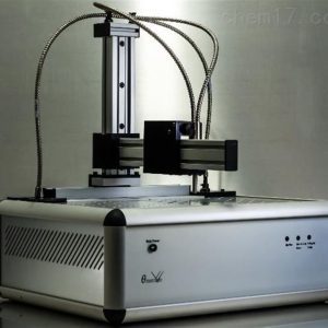

• Many applications: Can measure Si or III/V wafers with or without tape, with Film frame, bumped wafers, bonded wafer – with Si or Glass or Sapphire carriers, and many other materials.
• Not affected by tape thickness, adhesives, pattern structures or non conducting materials
• Non contact technique
• Fast- measurement speed about 1 second per point
• Easy recipe setup
• Easy interpretation of results
• Thickness
• Warpage
• Roughness
• Bump height
• Trench depth
• TSV depth
• Trim depth
By joining hands and leveraging cutting-edge technologies, we develop innovative solutions to drive societal progress and shape a better future.
With deep expertise and extensive experience, we deliver precise and efficient solutions to ensure every project meets the highest standards.
We integrate cutting-edge technology with continuous innovation to develop breakthrough solutions that drive industry progress and create lasting value for our clients.
We offer round-the-clock premium support services, ensuring rapid response and efficient problem resolution, allowing you to focus on your core business without worries.