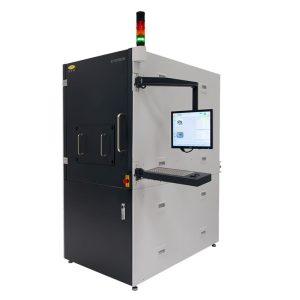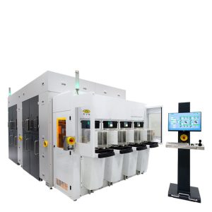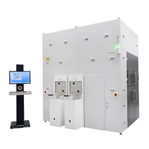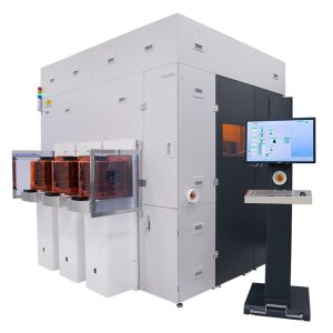

Vertical stacking of semiconductor devices has become an increasingly viable approach to enabling continuous improvements in device density and performance. Wafer-to-wafer bonding is an essential process step to enable 3D stacked devices. EVG’s GEMINI FB XT integrated fusion bonding system extends current standards and combines higher productivity with improved alignment and overlay accuracy for applications such as memory stacking, 3D systems on chip (SoC), backside illuminated CMOS image sensor stacking, and die partitioning. The system features the SmartView bond aligner, developed specifically for fusion and hybrid wafer bonding alignment requirements.
| Wafer diameter (substrate size) |
|---|
| 200, 300 mm |
| Max. number of process modules |
|---|
| 6 + SmartView® NT |
| Optional features |
|---|
| Debond module |
| Thermocompression bond module |
By joining hands and leveraging cutting-edge technologies, we develop innovative solutions to drive societal progress and shape a better future.
With deep expertise and extensive experience, we deliver precise and efficient solutions to ensure every project meets the highest standards.
We integrate cutting-edge technology with continuous innovation to develop breakthrough solutions that drive industry progress and create lasting value for our clients.
We offer round-the-clock premium support services, ensuring rapid response and efficient problem resolution, allowing you to focus on your core business without worries.