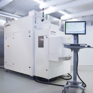

The microDICE laser micromachining system leverages TLS-Dicing (thermal laser separation) – a unique technology that uses thermally induced mechanical forces to separate brittle semiconductor materials, such as silicon (Si), silicon carbide (SiC), germanium (Ge) and gallium arsenide (GaAs), into dies with outstanding edge quality while increasing manufacturing yield and throughput. Compared to traditional separation technologies, such as saw dicing and laser ablation, TLS-Dicing enables a clean process, micro-crack-free edges, and higher resulting bending strength.
Capable of dicing speeds up to 300mm per second, the microDICE system provides up to a 10X increase in process throughput compared to traditional dicing systems. Its high throughput, outstanding edge quality and 300-mm wafer capable platform enables a true high-volume production process, especially for SiC-based devices.
In addition, microDICE reduces the dicing cost per wafer by up to an order of magnitude or more compared to other wafer dicing approaches. Due to the contactless laser machining method, there is no tool wear and no expensive consumables are required. This results in up to 15X lower cost of ownership over the entire life-time of the dicing system. microDICE also offers the ability to produce more dies per wafer by reducing the street width.
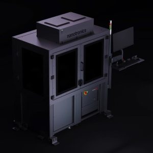
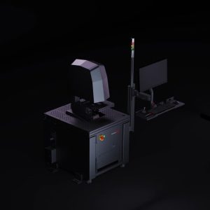
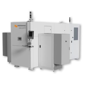
The microDICE standard system configuration consists of:
By joining hands and leveraging cutting-edge technologies, we develop innovative solutions to drive societal progress and shape a better future.
With deep expertise and extensive experience, we deliver precise and efficient solutions to ensure every project meets the highest standards.
We integrate cutting-edge technology with continuous innovation to develop breakthrough solutions that drive industry progress and create lasting value for our clients.
We offer round-the-clock premium support services, ensuring rapid response and efficient problem resolution, allowing you to focus on your core business without worries.