
OptoSurf developed the OptoScan 600 device especially to measure large semiconductor panels. Not only panels can be measured – the device can also be used for foils or flat parts like polished tools or mirrors.
The clean room capable OptoScan 600 can measure areas of maximum 600 x 600 mm². Different measurement programs are available: Line-scans in x- and y-orientation, partial and full scans, roughness analysis (Aq or – after creating a correlation – Ra, Rz), form and waviness. The system can be ordered with an additional vacuum chuck. Maximum feed rate is 600 mm/sec.
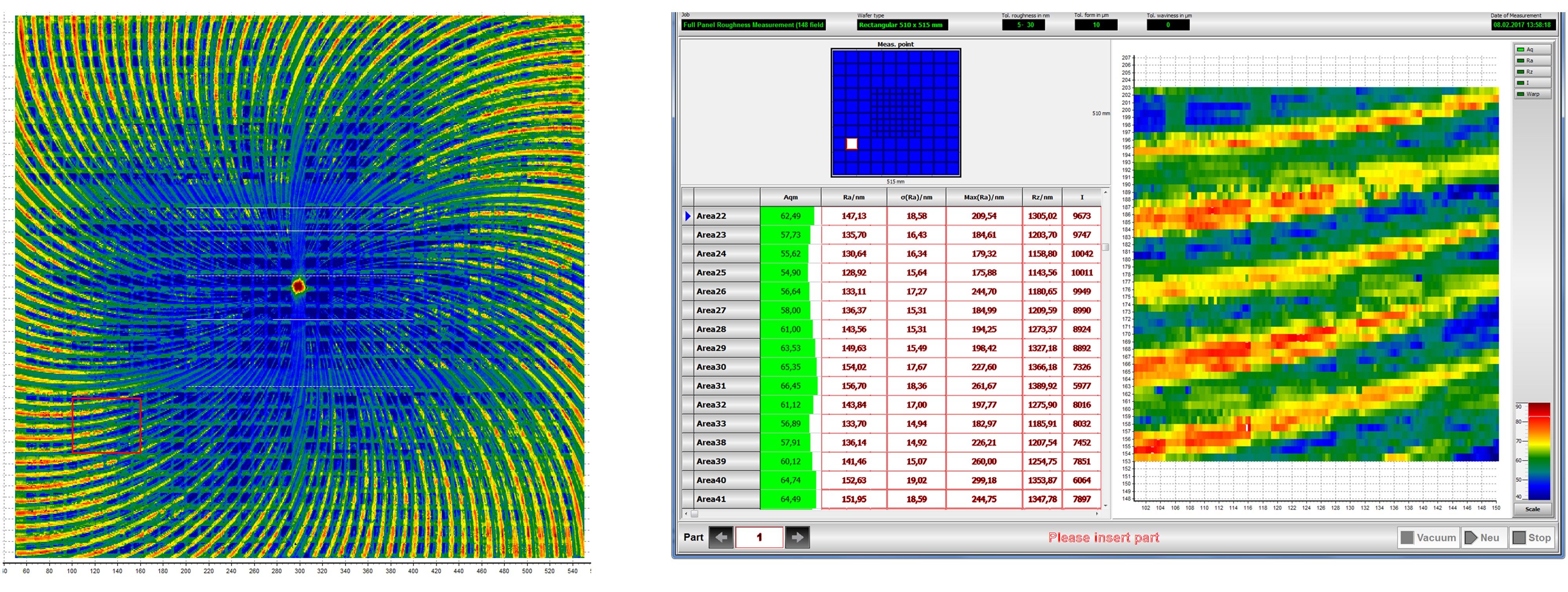
Example of usage in semiconductor technology. Measurement of panels with chips, which are finish ground after coating with mold. Left: roughness card of the whole surface (600 x 600 mm², Ra-values, scale from 0.09 µm – 0.2 µm). Right: an appraisal of 148 single segments. Graphic representation of segment 22