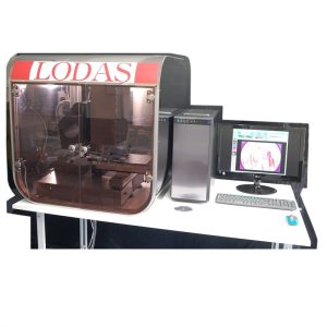

The UltraINSP Wafer Surface Defect Inspection System is the most comprehensive domestically developed product for surface defect detection. The system consists of four modules that enable full-surface wafer inspection and synchronized data acquisition, including: front-side, back-side, and edge defect inspection modules; profile, metrology, and inspection modules. It provides adaptive data acquisition control and innovatively utilizes measurement evaluation results to match multi-sensor fusion technology, ensuring high detection accuracy and stability. The system can replace imported defect inspection equipment to the greatest extent, offering significant economic benefits.
Edge Defect Inspection: Chipping, Corner Missing
Scribe Line Depth and Width Measurement
Chipping and Notch Detection on Scribe Lines
Excess Material Accumulation in Scribe Lines
Wire Bonding Quality Inspection
Solder Joint Quality Inspection
By joining hands and leveraging cutting-edge technologies, we develop innovative solutions to drive societal progress and shape a better future.
With deep expertise and extensive experience, we deliver precise and efficient solutions to ensure every project meets the highest standards.
We integrate cutting-edge technology with continuous innovation to develop breakthrough solutions that drive industry progress and create lasting value for our clients.
We offer round-the-clock premium support services, ensuring rapid response and efficient problem resolution, allowing you to focus on your core business without worries.